
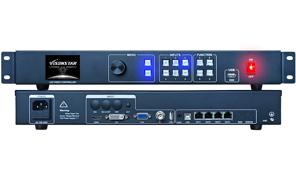
 VS Series
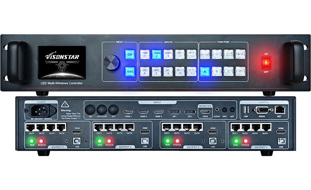 EX Series
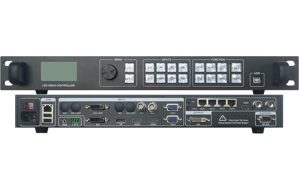 Multi-Windows Series
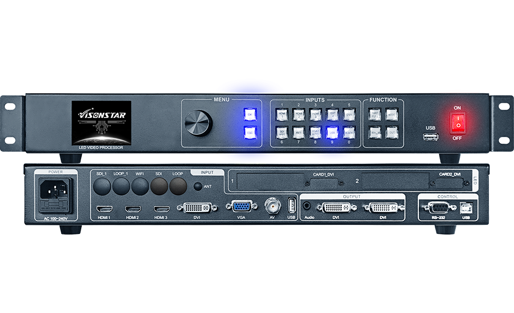 Video Processor
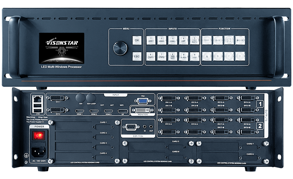 Video Splicer
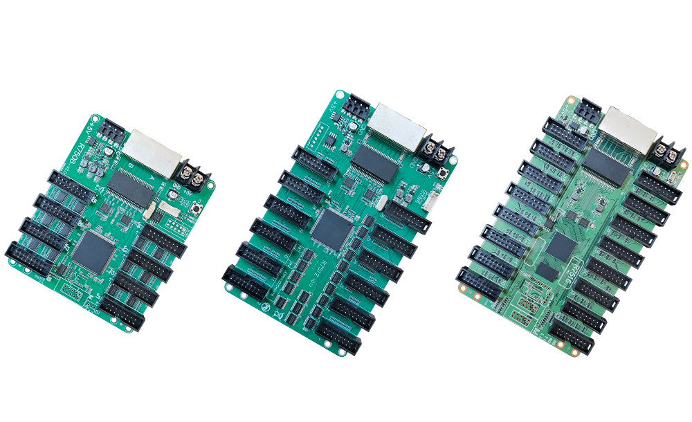 Receiving Card
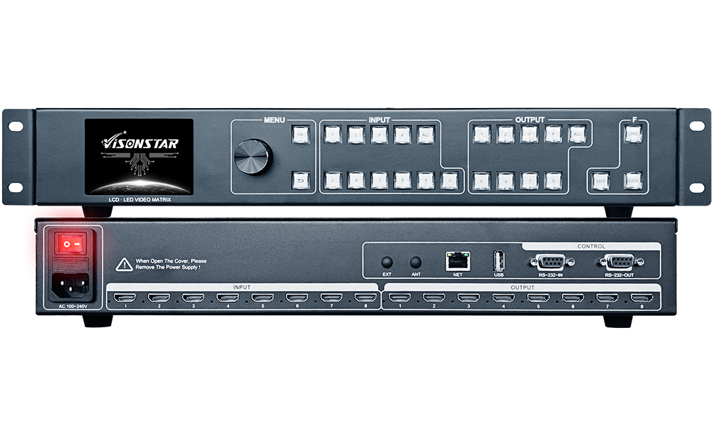 Video Matrix
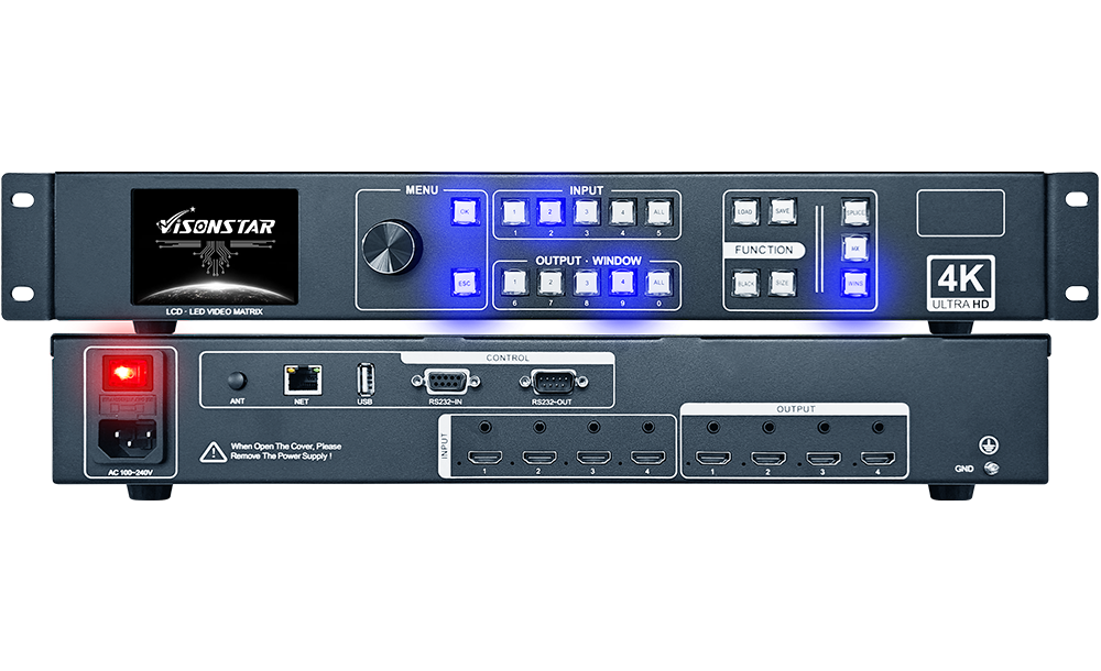 4K Matrix
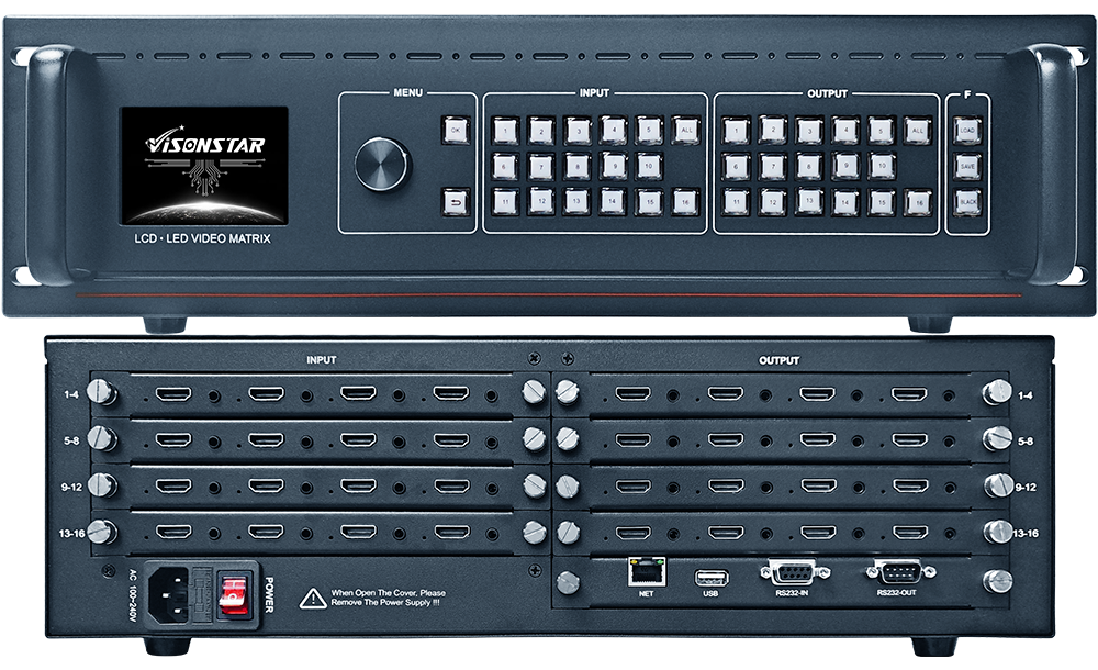 Plug-in Matrix
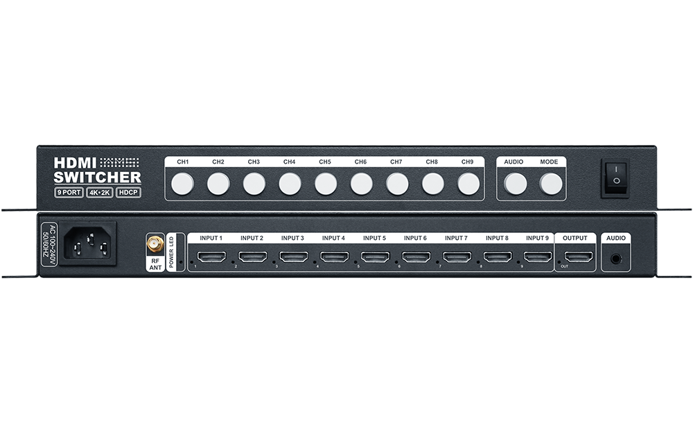 Multiviewer & Splicer
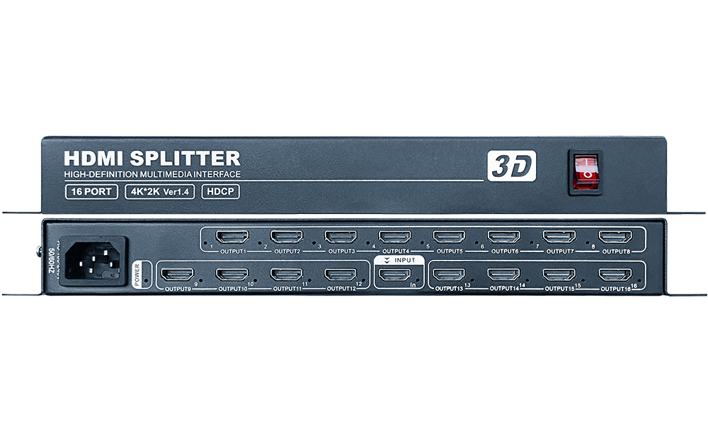 Signal Distributor
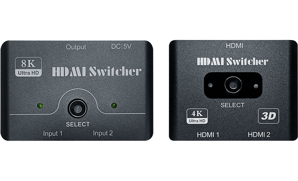 Signal Switcher
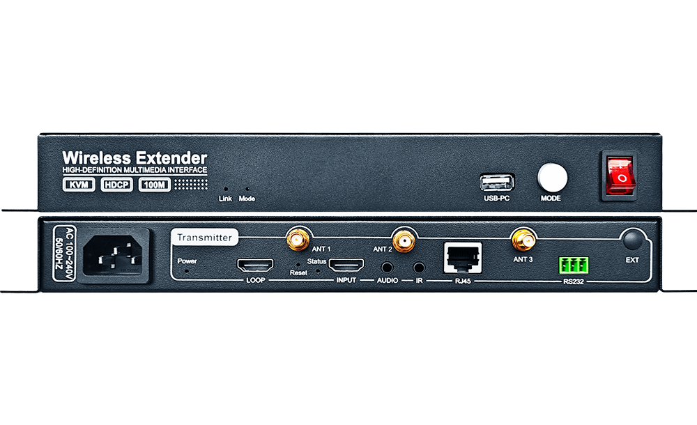 Wireless Extender
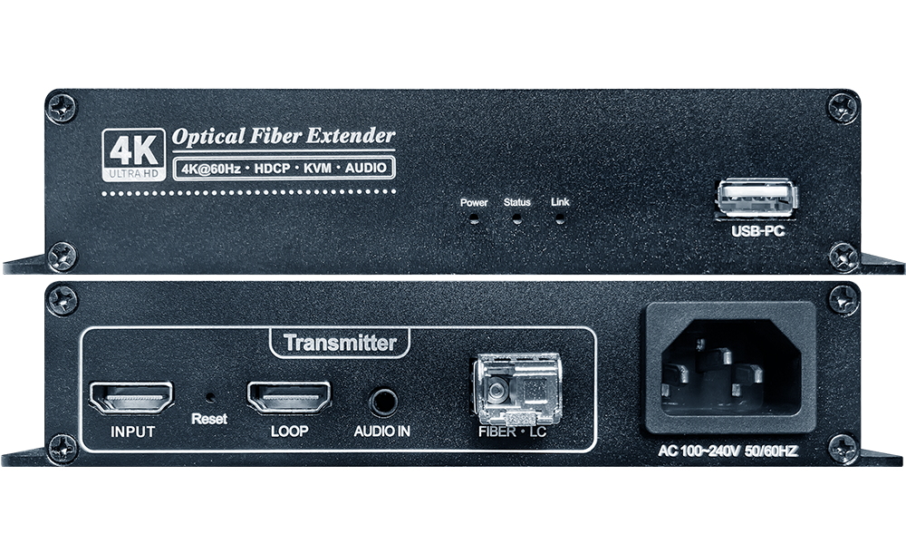 Optical Extender
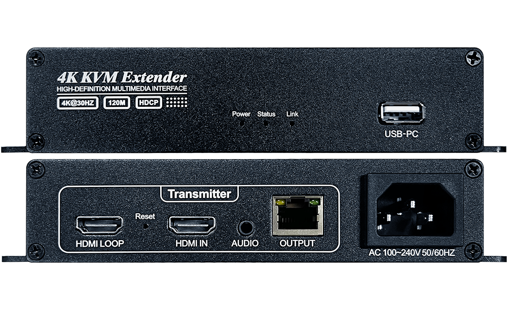 Network Extender
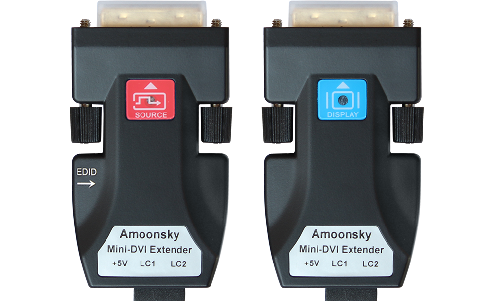 DVI Optical Extender
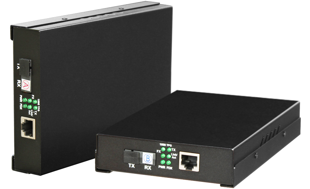 LED Optical Transceiver
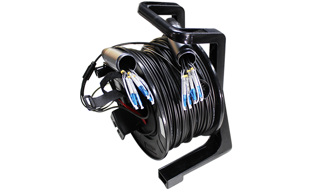 Optic Fiber
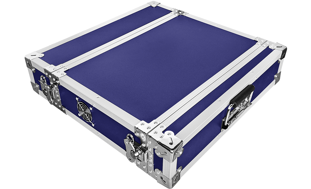 Flight Case
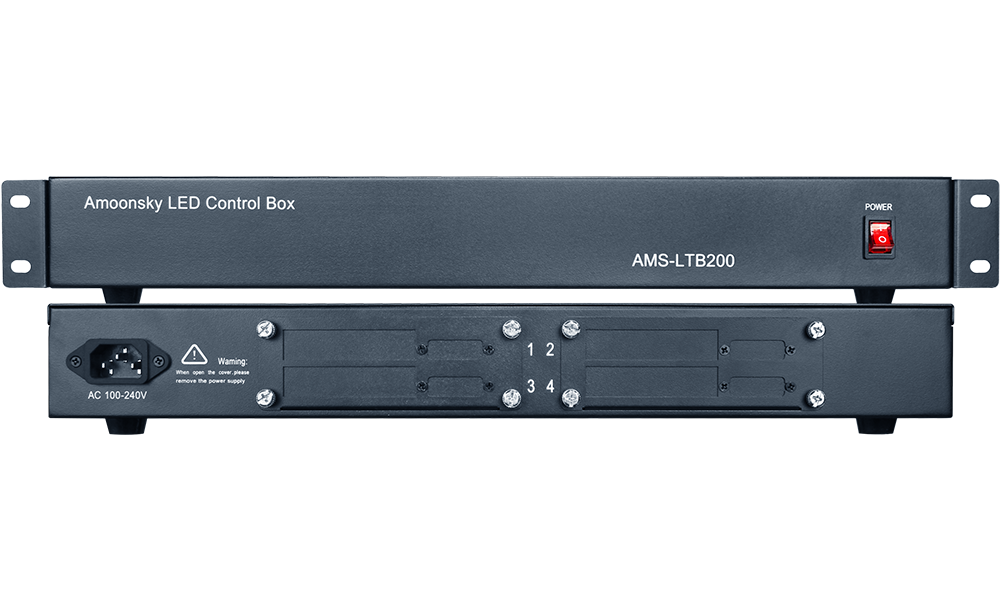 LED Sending Box
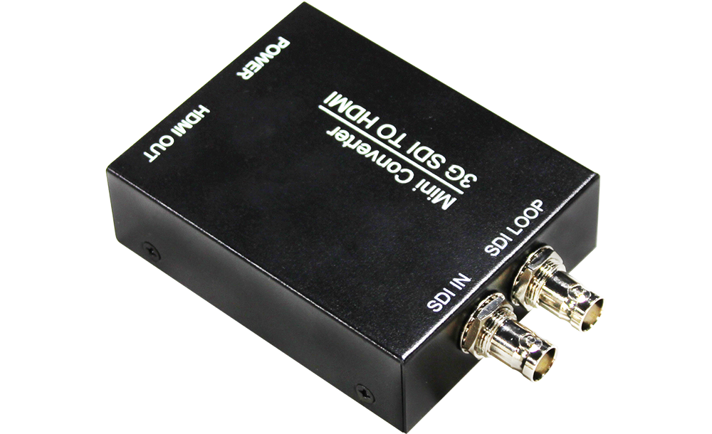 SDI Converter
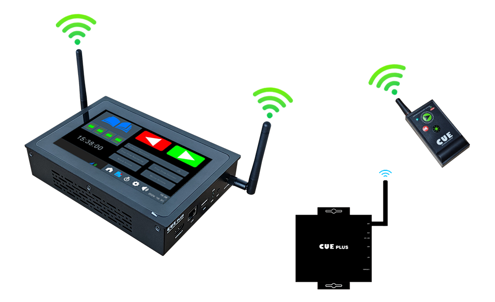 PPT Page Flipper And Timer
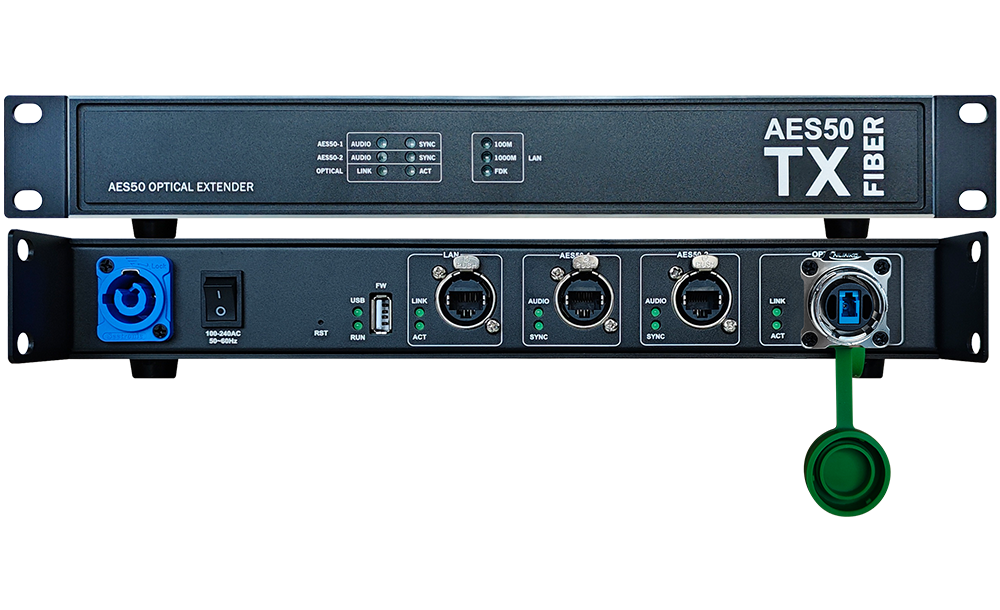 Dual Port Audio Fiber Optic Extender
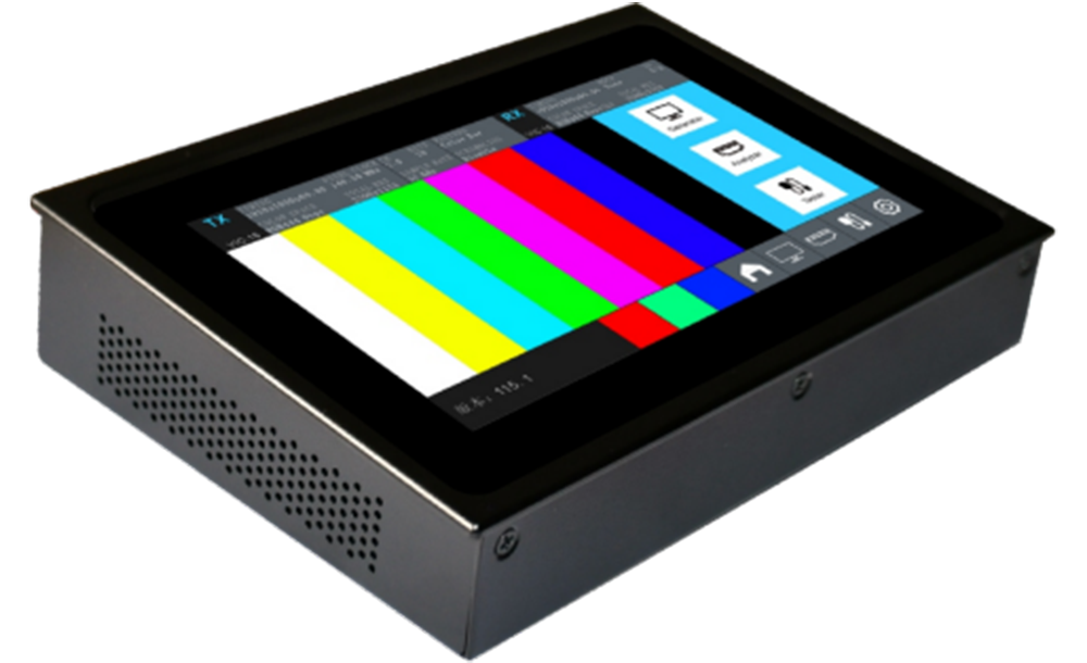 Signal Generator & Analyzer
 PCB Design
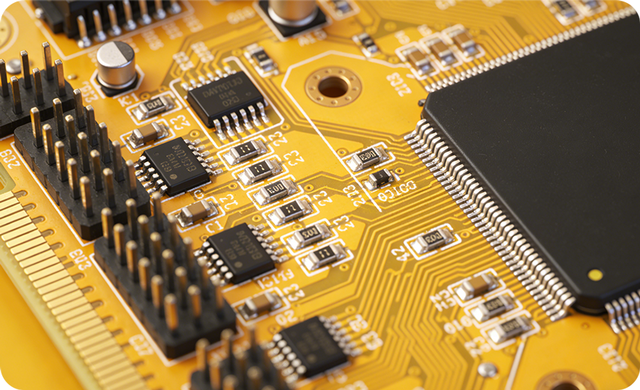 PCBA Design
 Scheme Design
Follow the full path from schematic capture and layout through manufacturability, assembly, inspection, testing, and production release.
Why PCBA design is a system
PCBA (Printed Circuit Board Assembly) design is far more than “connecting traces.” It involves DFM (Design for Manufacturability), DFT (Design for Testability), DFA (Design for Assembly), SI (Signal Integrity), PI (Power Integrity), Thermal Management, HDI (High-Density Interconnect), and EMC (Electromagnetic Compatibility). A well-executed PCBA design significantly reduces defect rates, testing costs, and rework risks while ensuring reliable electrical performance.
VISONSTAR provides professional hardware schematic design, high-density multi-layer PCB design, PCBA solution design, and product production support. This guide systematically covers the terminology and engineering practices used by hardware engineers, PCB layout engineers, NPI engineers, and procurement teams working with PCB design, PCBA design, PCB assembly, PCBA assembly, and PCBA reverse engineering for legacy products.
01
ENGINEERING CHAPTER
PCBA Design Flow and Key Input Output Files
PCBA design typically starts with Schematic Capture, followed by PCB Placement, Routing, DRC (Design Rule Check), and DFM Check, then outputs Gerber Files, NC Drill Files, BOM (Bill of Materials), and Assembly Drawing. For complex designs, HDI PCB technology with laser-drilled microvias and sequential lamination may be required.
Core input files include:
- Netlist
- Mechanical Drawing
- Component Datasheet
- Process Capability Document (minimum trace width/spacing, minimum hole size, solder mask dam width, impedance control requirements)
Core output files include:
- Gerber RS-274X or ODB++
- NC Drill File
- Pick & Place File
- Stencil Gerber
- Test Point Report
- Assembly Drawing & Silkscreen File
02
ENGINEERING CHAPTER
PCB Placement and Routing Core Rules for High Performance PCBA
2.1 Placement Principles
Placement is the foundation of PCBA design and directly affects Signal Routing Quality, Thermal Performance, and Manufacturability. Proper placement is critical for impedance control PCB designs and high-speed digital circuits.
- Functional Partitioning: Separate analog, digital, power, and high-speed interface areas to avoid interference.
- Signal Flow: Place components in the signal flow direction to reduce crossing and loop area.
- Critical Component Priority: Place MCU/FPGA/SoC, DDR, clock, and power modules first.
- Edge Placement: Connectors, buttons, and LEDs near board edges to meet mechanical requirements.
- Thermal Layout: High-power components near heat dissipation channels or thermal pads; add thermal via arrays under hot components.
2.2 Routing Essentials
- Trace Width & Current Capacity: 0.5 mm trace width on 1 oz copper carries approximately 1 A. For higher current, use copper pour or thicker copper weights.
- Differential Pair: USB, HDMI, LVDS, Ethernet require Length Matching, Equal Spacing, and Tight Coupling to maintain signal integrity and minimize insertion loss and return loss.
- Controlled Impedance: High-speed signals require characteristic impedance calculated from stack-up; common values are 50 Ω single-ended and 100 Ω differential. The engineering review should include impedance control verification.
- Return Path: Ensure a complete reference plane to avoid split plane EMI issues; add stitching vias near layer transitions.
- Via: Minimize high-speed vias; use Back Drilling or Blind/Buried Vias when necessary. For HDI designs, use stacked vias or staggered vias with copper filling.
03
ENGINEERING CHAPTER
DFM Design for Manufacturability The Key to Volume Production Yield for PCBA
Poor DFM leads to Solder Bridging, Tombstoning, Cold Solder Joints, Component Shift, and Solder Balls. DFM analysis before mass production helps protect first-pass yield.
3.1 Land Pattern Design
Land patterns must comply with IPC-7351. Proper pad design is essential for reliable PCB assembly and PCBA assembly.
- CHIP Components (0402, 0603, 0805): Pad size must match stencil aperture and reflow profile to avoid tombstoning.
- QFN (Quad Flat No-lead): The bottom Thermal Pad should be partitioned to reduce voiding and cold joints; use solder mask defined (SMD) or non-solder mask defined (NSMD) pads appropriately.
- BGA (Ball Grid Array): Pad diameter is typically 80–85% of ball diameter; solder mask opening must be precise to avoid solder mask on pad. For fine-pitch BGA, use solder mask dam width ≤0.1 mm or eliminate dam if needed.
- SOT/SOP/QFP: Fine pitch requires adequate solder mask dam width to prevent bridging.
3.2 Component Spacing & Orientation
- Adjacent component spacing must meet pick-and-place nozzle and rework requirements (≥0.3 mm).
- Align similar components in the same direction for easier AOI inspection.
- Keep sufficient distance between tall and short components to avoid shadow effect during reflow.
3.3 Solder Mask & Silkscreen
- Solder Mask Dam width ≥0.1 mm to prevent bridging.
- Silkscreen must not overlap pads; keep ≥0.2 mm clearance.
- Polarity Marking, Pin 1 Indicator, and Reference Designator must be clear.
- Choose solder mask color (green, blue, black, red, white) based on customer preference; ensure legend printing legibility.
04
ENGINEERING CHAPTER
DFT Design for Testability and DFA Design for Assembly Reliable PCBA Circuit Board Design
4.1 DFT
DFT enables efficient, low-cost PCBA testing and supports test program development and fixture design.
- Flying Probe Test: No fixture required; ideal for prototypes and small batches.
- ICT (In-Circuit Test): Requires test points and fixture; suitable for high volume. We design test point patterns with adequate coverage.
- FCT (Functional Circuit Test): Verifies actual PCBA functionality.
- Boundary Scan (JTAG): Uses built-in chip test logic to reduce physical test points.
DFT requirements:
- Test point diameter ≥0.8 mm, spacing ≥1.27 mm.
- Distribute test points on one side when possible.
- Keep test points unobstructed and away from tall components.
- Reserve test points for power and ground nets to enable power-off short test and power-on voltage measurement.
4.2 DFA
DFA focuses on assembly efficiency and error prevention.
- Panelization: Use V-cut (V-Scoring) or Mouse Bite / Stamp Hole. For pcb assembly with edge-hanging components, use tab routing with mouse bites.
- Tooling Rail: 3–5 mm wide for conveyor transfer and positioning.
- Fiducial Mark: At least 2–3 global fiducials; local fiducials for fine-pitch devices like BGA and QFN.
- Poka-Yoke: Ensure connectors have unique orientation to prevent reverse insertion.
05
ENGINEERING CHAPTER
High Speed and High Frequency Design Signal Integrity Power Integrity EMC and HDI PCB Techniques
5.1 Signal Integrity (SI)
SI issues include Reflection, Crosstalk, Overshoot, Undershoot, and Timing Skew. High-speed PCB design can use pre-layout simulation and post-layout verification to evaluate the eye diagram.
- Impedance Matching: Source series termination, parallel termination, or AC termination.
- Length Matching: Serpentine routing for DDR data/address groups and differential pairs.
- Crosstalk Suppression: 3W rule (spacing ≥3× trace width); add guard traces for critical signals.
- Return Via: Add stitching vias near layer transitions to reduce loop inductance.
5.2 Power Integrity (PI)
PI issues include Power Noise, Voltage Drop, and Ground Bounce. A well-designed Power Distribution Network (PDN) is critical for stable operation.
- Decoupling Capacitor: Place 0.1 µF + 10 µF combinations near each power pin; use low-ESL capacitors for high-frequency decoupling.
- Power Plane Split: Separate analog and digital power planes; avoid crossing splits with high-speed signals.
- Low Impedance Path: Adjacent power and ground planes create plane capacitance; maintain thin dielectric between power and ground layers.
- Via Count: Parallel multiple vias for high-current paths; use copper-filled vias for high-current vias.
5.3 EMC (Electromagnetic Compatibility)
EMC covers EMI (Electromagnetic Interference) and EMS (Electromagnetic Susceptibility). An EMC pre-compliance review can identify design risks before formal testing.
- 20H Rule: Recess power plane edges by 20× layer spacing to reduce fringing fields.
- Interface Filtering: Add TVS, common mode chokes, ferrite beads, and capacitors at I/O connectors.
- Shielding: Use shielding covers over sensitive areas; provide grounding pads for shield attachment.
- Crystal & Clock: No routing under crystals; use guard traces and keep clock traces short.
5.4 HDI PCB Design
For high-density designs, HDI PCB technology with laser-drilled microvias, blind vias, and buried vias enables smaller form factors and higher routing density. Key considerations:
- Microvia aspect ratio typically ≤1:1.
- Use stacked microvias for layer transitions in high-density areas.
- Sequential lamination process allows multiple microvia layers.
- Via-in-pad with copper filling and planarization for BGA fanout.
06
ENGINEERING CHAPTER
Package and Pad Design Deep Dive for BGA and QFN PCBA
6.1 BGA Design
BGA pad design directly affects soldering yield for PCB assembly and PCBA assembly, especially in fine-pitch BGA applications.
- Pad diameter ≈0.8–0.85× ball diameter (e.g., 0.25 mm pad for 0.3 mm ball).
- Solder mask opening larger than pad by 0.025–0.05 mm per side.
- NSMD (Non-Solder Mask Defined) or SMD (Solder Mask Defined); NSMD common for fine-pitch BGA.
- Fanout vias 0.2 mm/0.1 mm or smaller; use Via-in-Pad with Copper Filled / Resin Filled to prevent solder wicking.
- Add local fiducial marks near BGA for accurate placement.
6.2 QFN Design
QFN (Quad Flat No-lead) packages require careful thermal pad design.
- Partition thermal pad into multiple smaller pads or use a single pad with segmented stencil apertures to reduce voiding.
- Extend pin pads 0.2–0.3 mm beyond package edge for AOI inspection.
- Use Resin Plugging or Copper Filling for thermal pad vias to prevent solder wicking.
- For high-power QFN, add thermal via array connecting to internal copper planes.
6.3 0402 / 0201 / 01005 Micro Components
- 0402 pad spacing: 0.4–0.5 mm; 0201: 0.25–0.3 mm; 01005: 0.15–0.2 mm.
- Use anti-solder ball stencil apertures (notched or reduced).
- Provide sufficient fiducial marks for placement accuracy.
- Consider glue dispensing for double-sided assembly with heavy components.
07
ENGINEERING CHAPTER
Stencil Design and Soldering Process for High Yield PCBA Assembly
7.1 Stencil Aperture Design
Stencil aperture design directly determines solder paste printing quality and should be optimized for each PCBA.
- Stencil Thickness: 0.1–0.15 mm typical; 0.08 mm for micro components; 0.2 mm for high current.
- Area Ratio: Aperture area / aperture wall area > 0.66.
- Aspect Ratio: Aperture width / stencil thickness > 1.5.
- Special Apertures: QFN thermal pad multiple small windows; BGA circular or square reduction; anti-solder ball notched apertures for chip components.
- Consider step stencil for mixed component sizes (e.g., thick stencil for high-current areas, thin for fine-pitch).
7.2 Reflow & Wave Soldering
- Reflow Soldering: For SMT components; requires proper temperature profile (preheat, soak, reflow, cooling). Use nitrogen reflow for improved wetting and reduced oxidation.
- Wave Soldering: For through-hole (DIP) components and SMT red glue process.
- Selective Wave Soldering: Localized soldering for through-hole components; ideal for mixed-technology boards.
- Lead-Free Process: SAC305 solder paste; peak reflow temperature 235–250 °C. Common surface finishes include lead-free HASL, ENIG, OSP, immersion silver, and immersion tin.
7.3 Mixed Assembly
Combine SMT reflow and DIP wave soldering, or use Pin-in-Paste (PIP) for through-hole components in reflow.
08
ENGINEERING CHAPTER
Panelization and Tooling Rail Boosting Production Efficiency for PCB Assembly
8.1 Panelization Methods
- V-cut (V-Scoring): Low cost; for rectangular boards without edge components.
- Mouse Bite / Stamp Hole: For irregular boards or edge components; use tab routing with mouse bites.
- Bridge + Mouse Bite: Combines strength and separation ease.
8.2 Tooling Rail & Fiducial Mark
- Tooling rail width: 3–5 mm.
- Fiducial mark: 1 mm diameter, 2–3 mm solder mask opening, gold or immersion tin finish.
- Local fiducials for BGA/QFN fine-pitch devices.
8.3 Panel Size & Quantity
- Panel size within pick-and-place and reflow oven limits (≤400 mm × 400 mm).
- Balance efficiency and material utilization; avoid warpage.
- Use breakaway tabs or routed slots to reduce stress during depaneling.
09
ENGINEERING CHAPTER
Output Data and Review Checklist for PCBA Design
9.1 Electrical Check
- DRC no fatal errors.
- Critical signal length matching, impedance, spacing.
- Power net via count and current capacity.
- Signal integrity simulation results meet eye diagram requirements.
9.2 DFM Check
- Pad size per IPC-7351.
- Component spacing meets minimum pick-and-place requirements.
- Solder mask dam, silkscreen, polarity marking clear.
- Stencil aperture meets area ratio.
- Panelization and tooling rail present.
9.3 DFT Check
- Test point coverage on critical nets.
- Test points unobstructed.
- ICT fixture feasibility.
9.4 Assembly Check
- Tooling rail and fiducial marks present.
- Panelization method reasonable.
- Component distance from V-cut ≥0.5 mm.
9.5 Documentation Completeness
- Gerber layer naming standardized.
- BOM part numbers, packages, quantities accurate.
- Pick & place file matches BOM.
- Stencil file matches PCB design.
10
ENGINEERING CHAPTER
PCBA Reverse Engineering and Value Added Services
For legacy products or obsolete PCBA circuit boards, PCBA reverse engineering can recreate schematics, BOM, and Gerber files from physical boards and connect the recovered data to a new PCB design and PCBA assembly workflow.
Our reverse engineering process includes:
- Board imaging and X-ray inspection to map internal layers.
- Component identification and BOM extraction including obsolete part replacements.
- Schematic capture from netlist reconstruction.
- PCB layout recreation with DFM improvements.
- Prototype PCBA assembly and functional testing.
Additional value-added services:
- Conformal coating for harsh environments.
- Potting and encapsulation for vibration resistance.
- Underfill for BGA and CSP packages.
- Rework and repair using BGA rework station.
- Functional test development for custom PCBA.
11
ENGINEERING CHAPTER
Common PCBA Design Errors and Avoidance Strategies
| Common Error | Consequence | Avoidance Strategy |
|---|---|---|
| Undersized Land Pattern | Cold Solder Joint, Tombstoning | Follow IPC-7351 Standard |
| Missing Solder Mask Dam | Solder Bridging | Maintain Dam Width ≥0.1mm |
| Insufficient Test Points | ICT Coverage Gap | Reserve Test Points on Critical Nets |
| Differential Pair Length Mismatch | Signal Distortion | Perform Length Matching (Serpentine) |
| Decoupling Capacitor Too Far | High Power Noise | Place Close to Power Pin |
| Insufficient Vias for High Current | Overheating, Voltage Drop | Parallel Multiple Vias |
| No Tooling Rail on Panel | Cannot Auto-SMT | Add Tooling Rail & Fiducial Mark |
| Component Too Close to V-cut | Damage During Depanel | Maintain Safe Spacing |
| Missing Thermal Relief on Large Copper | Soldering Difficulty | Add Thermal Relief Pads |
Conclusion
Electrical Performance Manufacturing Test and Assembly Designed Together
PCBA design is a systematic engineering discipline that integrates electrical performance, manufacturing processes, test strategies, and assembly efficiency. Mastering DFM, DFT, DFA, Signal Integrity, Power Integrity, Thermal Management, HDI PCB techniques, and EMC helps engineers reduce design iterations and improve volume production yield.
VISONSTAR’s PCBA scope includes professional hardware schematic design, high-density multi-layer PCB design, PCBA solution design, and product production support. A disciplined workflow from PCB design through PCB assembly, PCBA assembly, and verification helps convert engineering intent into a reliable production package.
Frequently asked questions
Six Practical PCBA Answers
01What is the difference between PCB and PCBA?
PCB is a bare printed circuit board; PCBA is a printed circuit board assembly with components mounted.
02What does a DFM check typically include?
Pad design, component spacing, solder mask dam, silkscreen, stencil aperture, panelization, tooling rail, fiducial marks, and wave soldering direction.
03What are the most common BGA pad design mistakes?
Incorrect pad diameter, solder mask opening offset, unfilled fanout vias causing solder wicking, and missing local fiducials.
04How to choose stencil thickness?
0.1–0.12 mm for standard SMT; 0.08 mm for 0201/01005; 0.15–0.2 mm for high current; verify with area ratio.
05What files are needed for PCBA manufacturing?
Gerber files, NC drill file, pick & place file, BOM, assembly drawing, stencil file, test point report, and optionally ODB++.
06What is HDI PCB?
HDI (High-Density Interconnect) PCB uses laser-drilled microvias, blind/buried vias, and sequential lamination to achieve higher routing density and smaller form factors.